Building an 8088 Computer from Scratch
Acknowledgment: This project was completed as part of a computer systems course taught by Dr. Kevin Angstadt at St. Lawrence University. The system blueprint and guidance that made this project possible can be found on Dr. Angstadt’s website.
Introduction
In this post I will talk through one of the coolest projects I have been a part of, building a computer from the ground up. Wiring individual chips on a breadboard, connecting a CPU to memory, and watching your creation execute its first instruction. Over the course of several weeks, I did exactly that: constructed a functional 8088-based computer capable of running programs, displaying output on an LCD, and booting from persistent storage. This post details the hardware journey from naked breadboard to working computer, detailing each component added and the functionality it enabled. By the end, the computer could perform a power-on self-test (POST), boot from a CompactFlash card, and communicate with a modern PC through a serial connection.
Power Distribution System
The first thing any computer needs to run is power, so my first step was preparing the breadboard’s power rails. Breadboards have separate rail segments, but for consistent power delivery, I connected all VCC (power) rails together and all ground rails together. I scattered capacitors evenly across the board, which smooth out minor voltage fluctuations and maintain stable direct current to all components.
 Before proceeding, I tested for short circuits by passing current through the board and measuring the return. Since no positive and negative paths should connect yet, the returning current should be zero, and it was. The breadboard was all powered up.
Clock Signal
Clock signals synchronize hardware operations in the computer acting as a steady pulse that drives each instruction cycle. I play piano so I like to think of it as using a metronome to make sure your playing on the correct beat. I built a clock circuit using an oscillator, a clock generator chip, and supporting components including a capacitor and resistor. The design produced a 33% high, 66% low duty cycle clock signal. I also added a reset button to the circuit. This allows the computer to restart without disconnecting power which is very useful for testing and debugging.
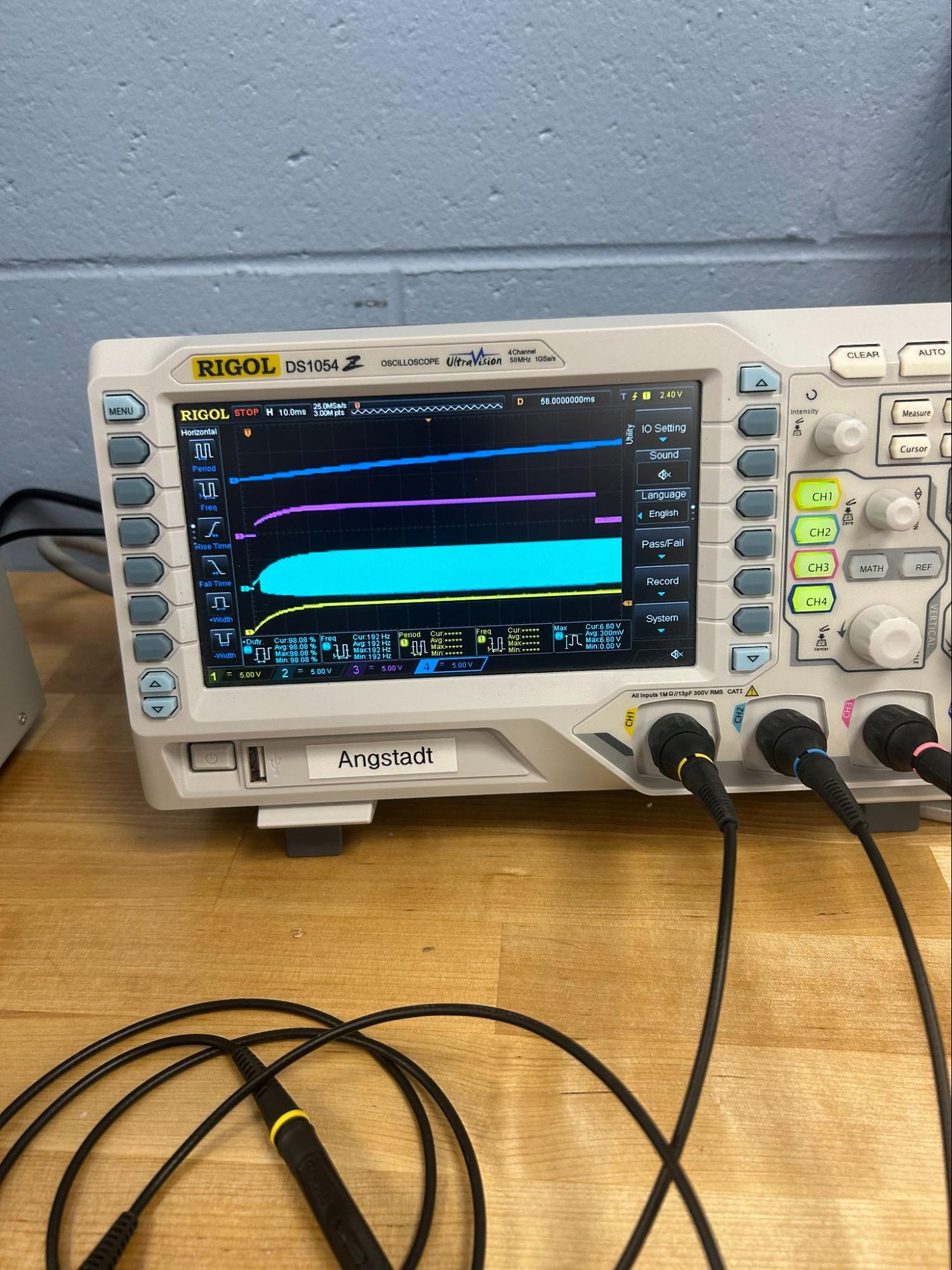
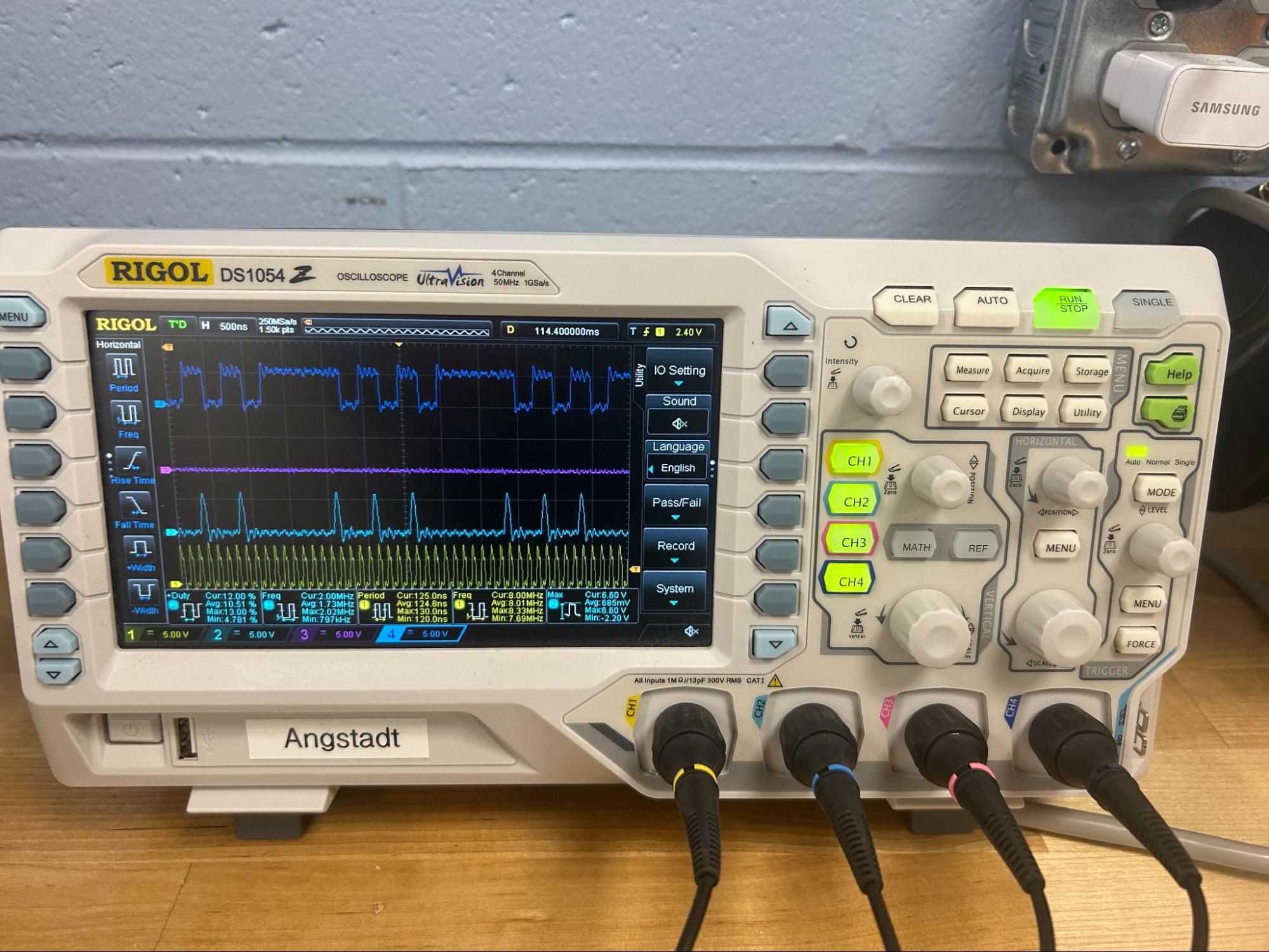
To verify the clock worked correctly, I connected the board to an oscilloscope. The output showed exactly what we wanted: a clean clock signal with the correct duty cycle. When holding the reset button, the reset signal responded appropriately.
CPU and Support Chips
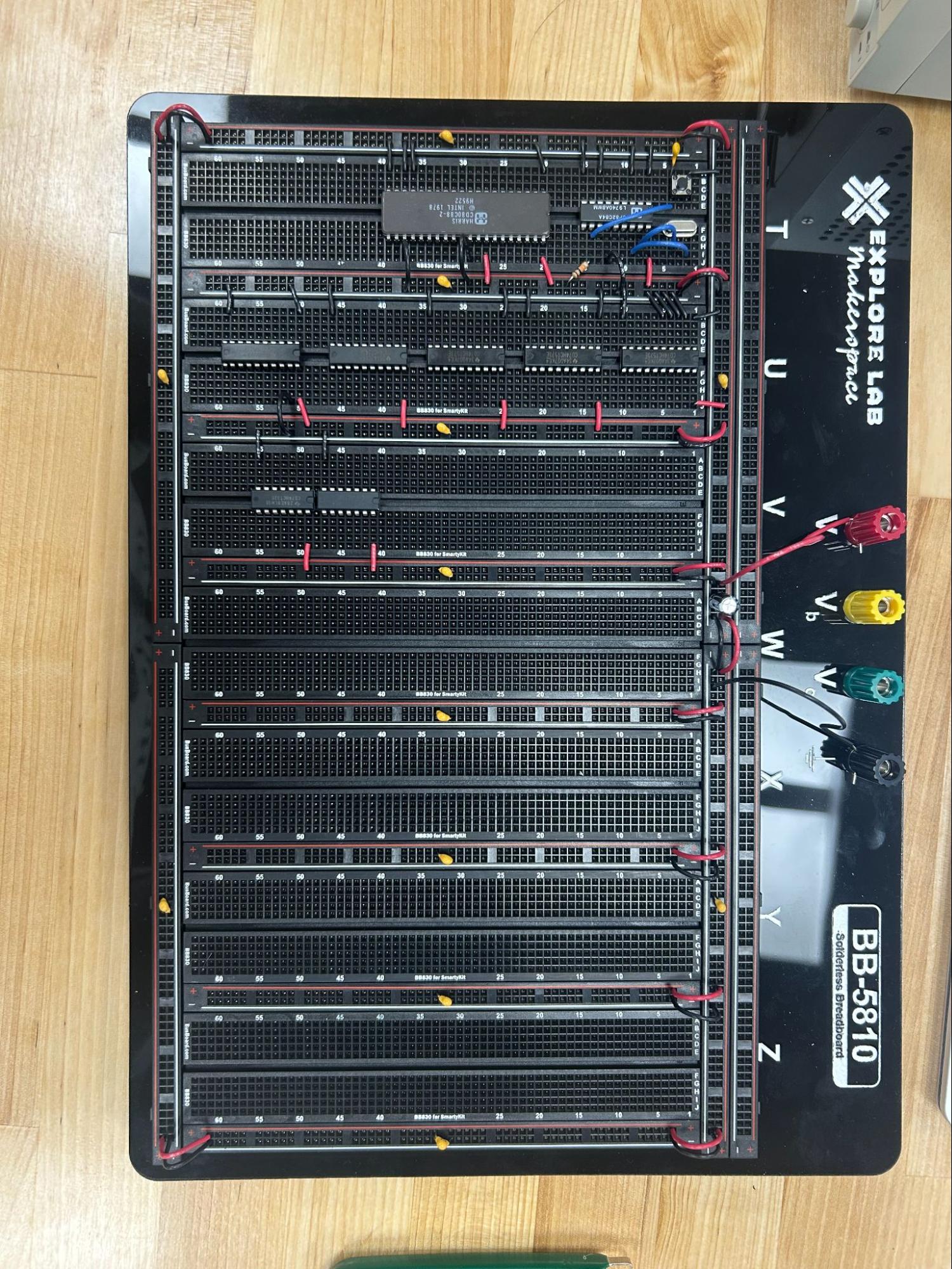
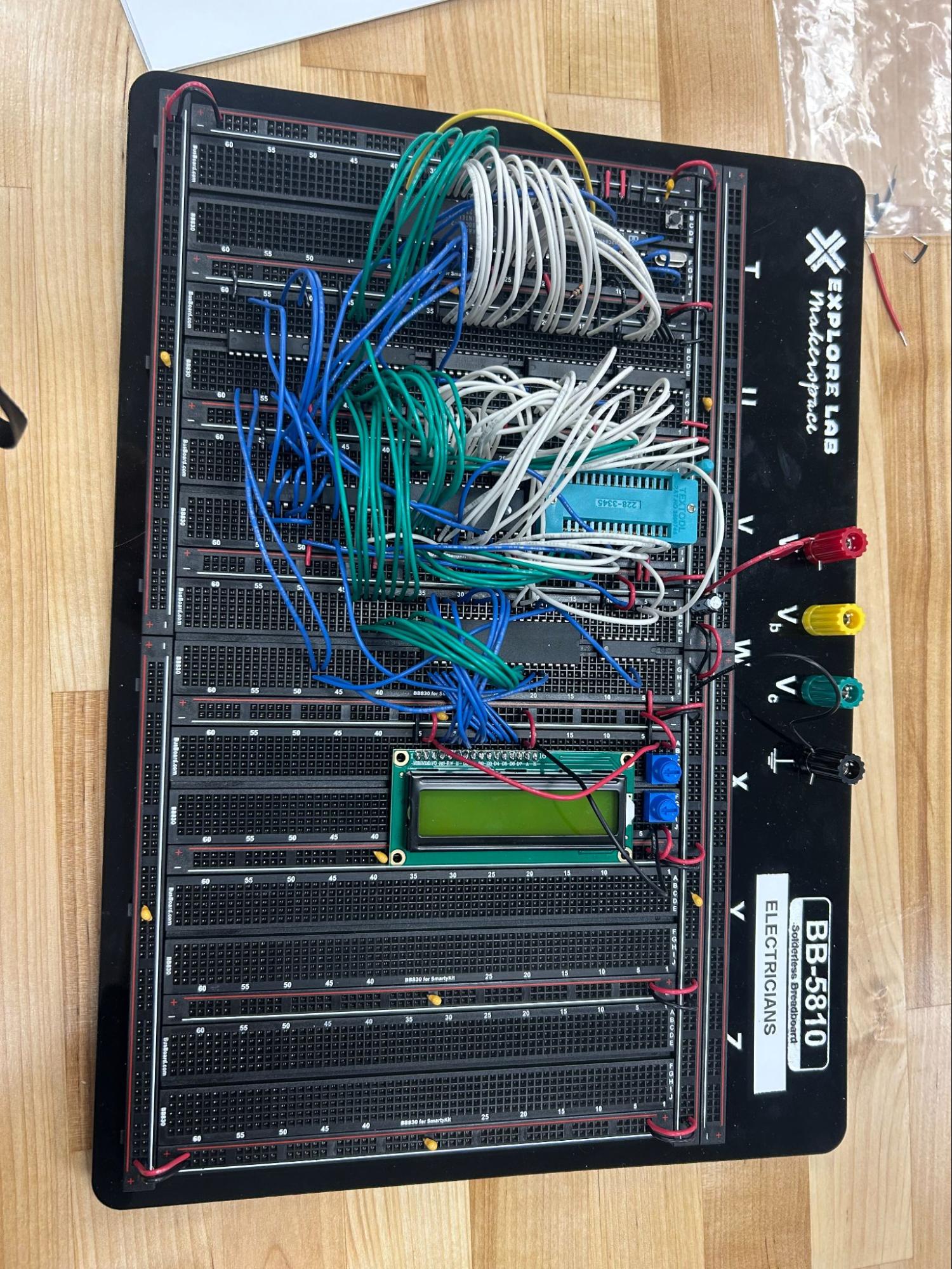
With stable power and a clock signal, it was time to install the Intel 8088 processor. The 8088 uses the same pins to operate with both data and address, so I needed to add latches to hold address information while data operations execute. I also installed a buffer to manage read/write data and a bus transceiver to enable data transfer between different parts of the system.
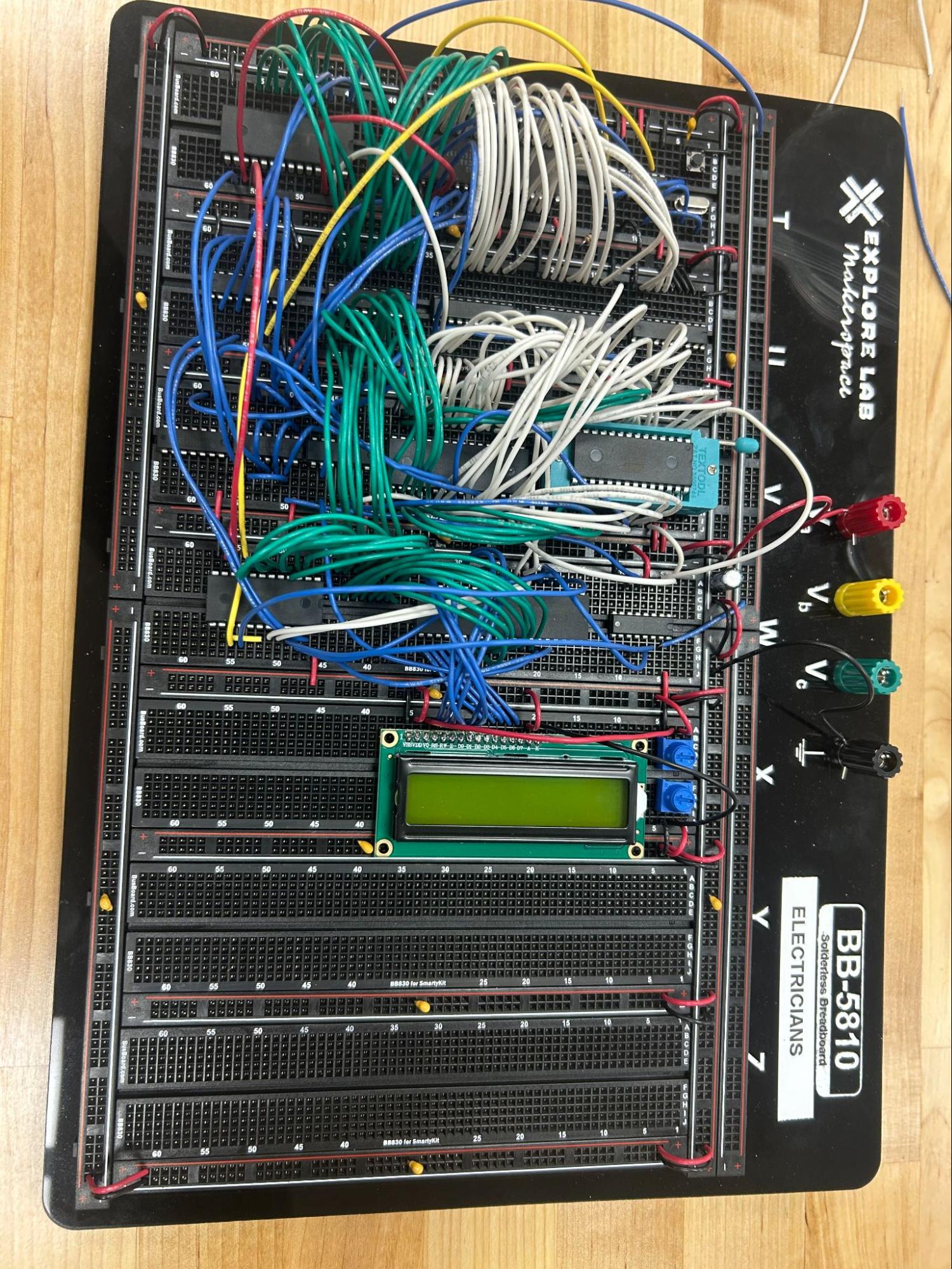
After placing the chips, I wired ground and VCC connections to power each component, then added signal wires (blue) to enable communication between chips. Next came the crucial connections: address wires (white) to route information to the correct destinations, data wires (green) to carry actual information between components, and a yellow wire to deliver the clock signal to the processor.
Memory
A processor needs somewhere to store instructions and data, so I set up two types of memory: RAM (Random Access Memory) for volatile storage at addresses 0x00000 to 0x7FFFF, and ROM (Read Only Memory) for non-volatile program storage at addresses 0xF8000 to 0xFFFFF. The ROM sits at the top of the memory space, which is where the 8088 looks for its first instruction when powered on.
To determine whether an address refers to RAM or ROM, I used a simple inverter that checks if the address is above or below 0x80000. I also installed a ZIF (Zero Insertion Force) adapter for the ROM chip to make it easy to add and remove to the system since I was constantly writing new programs to it from another computer.
After adding all the necessary signal, address, and data wires to connect memory to the rest of the system, I had a functional computer.
Testing the System
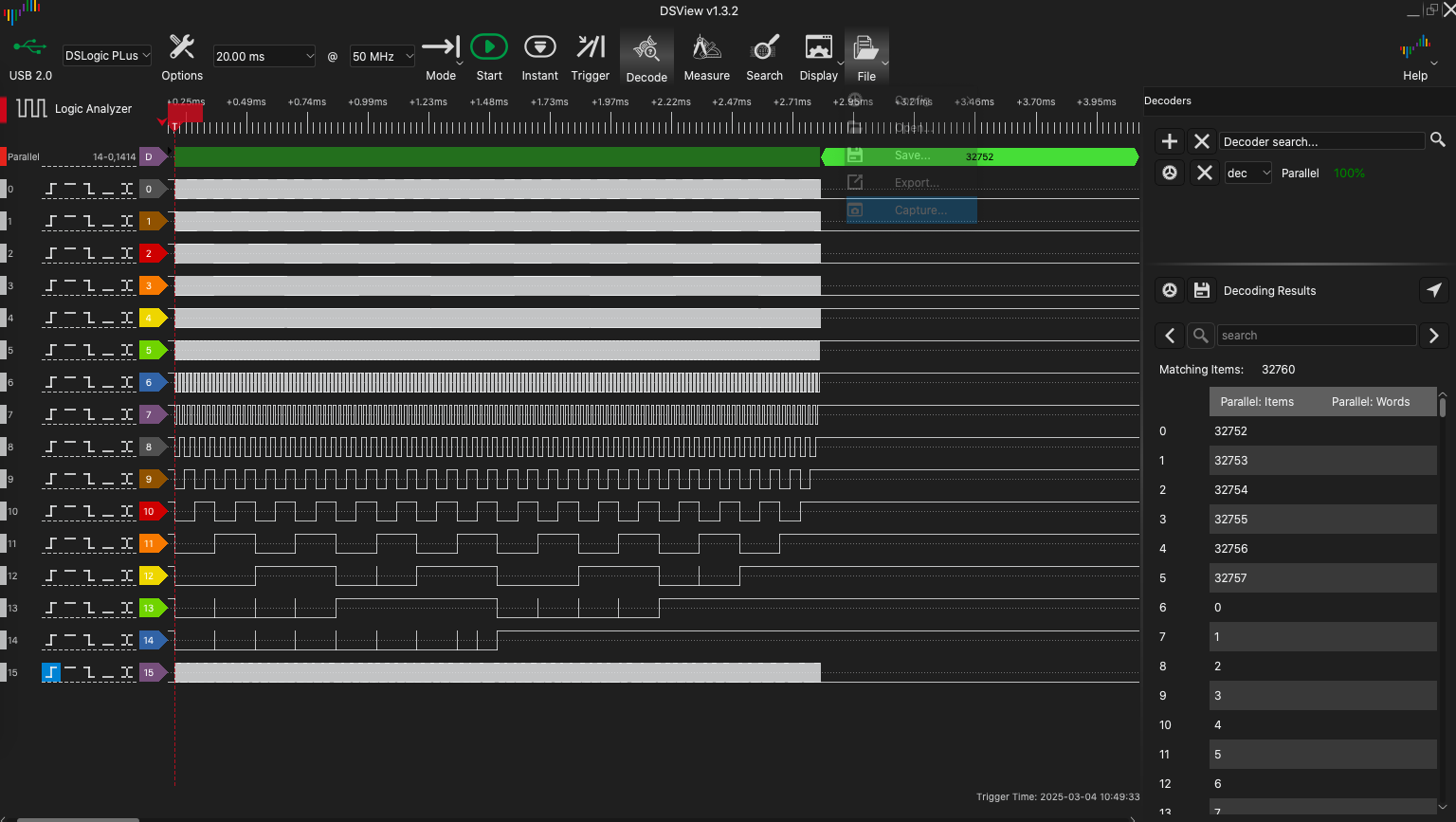
Back at the oscilloscope station, I probed various signals to verify everything worked. The output showed the memory read signal, reset button signal, first data bit, and clock signal all behaving correctly. When I pressed reset, the signals responded as expected. The computer was now capable of executing programs. I aslo want to ensure the address wires were appropriately connected to the rom by using a logic analyzer, which displays signals from the address wires to the ROM pins. I downloaded the data from the logic analyzer, which is just a list of numbers that should be in order from 0 to 2^15 - 1. I then wrote a quick python loop to output the same numbers, and ran both sets of data through a difference checker to ensure the data from the logic analyzer was correct, which it was.
I/O vs Memory
With a working bare-bones computer, the next step was adding input/output capabilities. I/O and memory have separate address spaces but are accessed using different commands. On the 8088 cpu, the designated address space is for I/O devices is 16 bits, so the range of ports (I/O addressed) is 0x0000 to 0xFFFF and can be accessed using IN and OUT instructions. The memory on the other hand is 20 bits 0x00000 to 0xFFFFF and is accessed using other commands such as mov. To allow the computer to read and write to I/O devices, I needed to separate read and write controls, then send the command to correct I/O device given port information. I used a decoder that received an address and instructions to enable the correct feature.
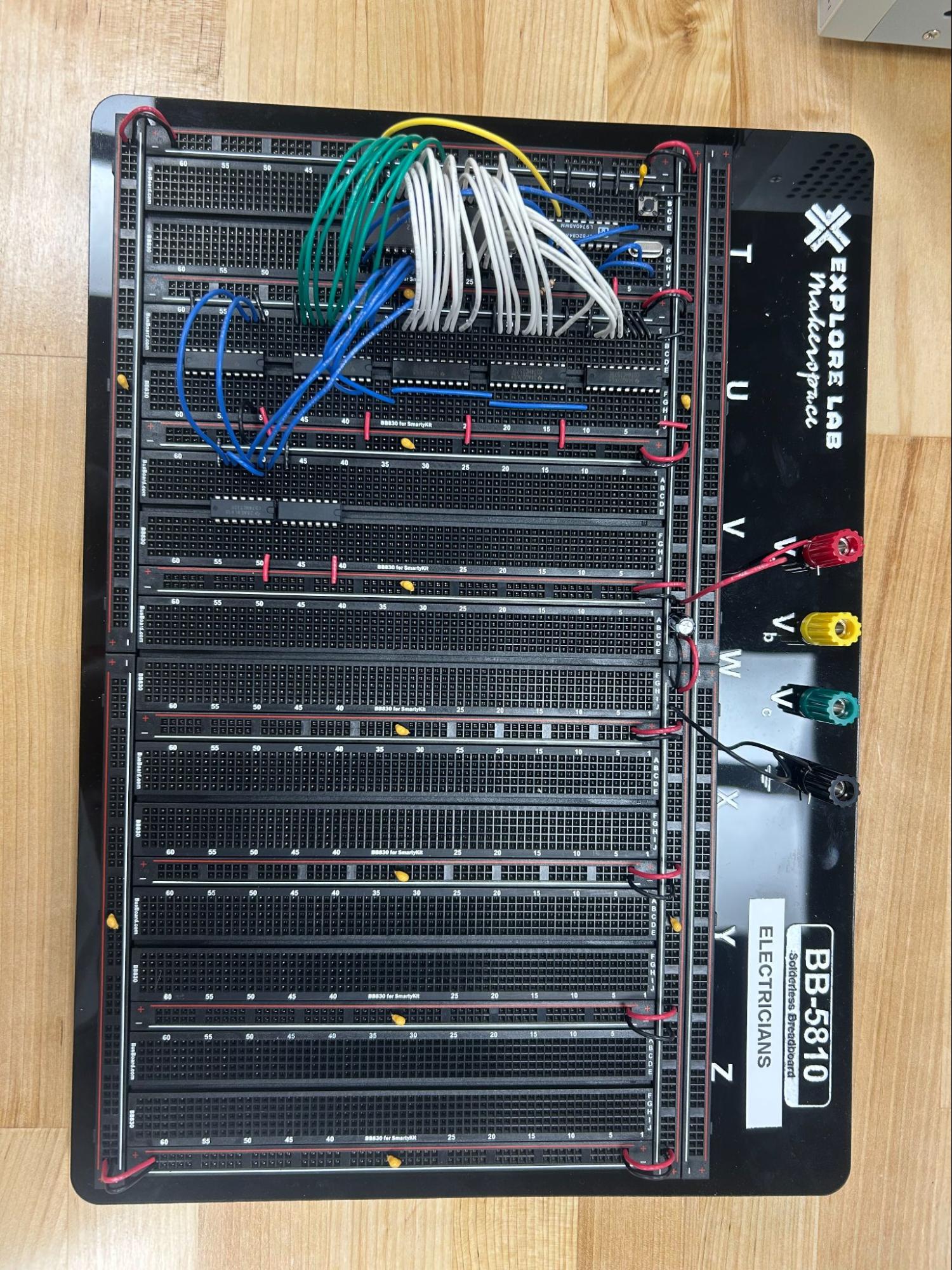
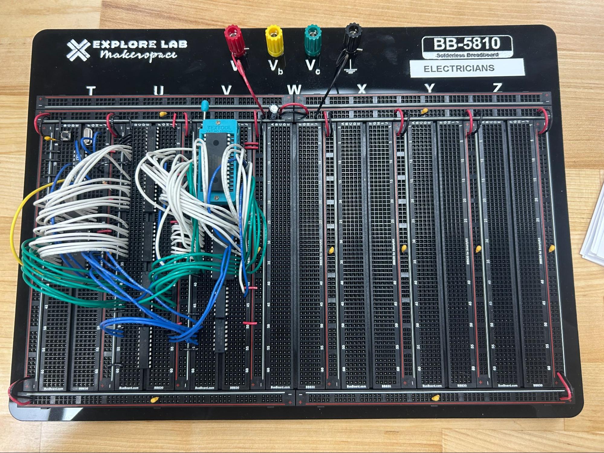
LCD Hardware
I inserted a decoder chip and a PIO (Programmable Input/Output) chip that allows the CPU to communicate with I/O devices. Then came the LCD itself, along with a couple of resistors and the usual power and ground connections. I wired numerous signal, address, and data connections between the memory, CPU, and LCD. These wires carry LCD instructions, character data, and control signals that make the display function.
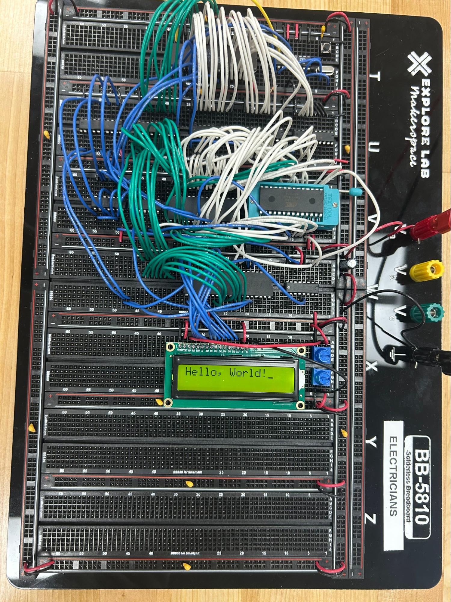
“Hello, World”
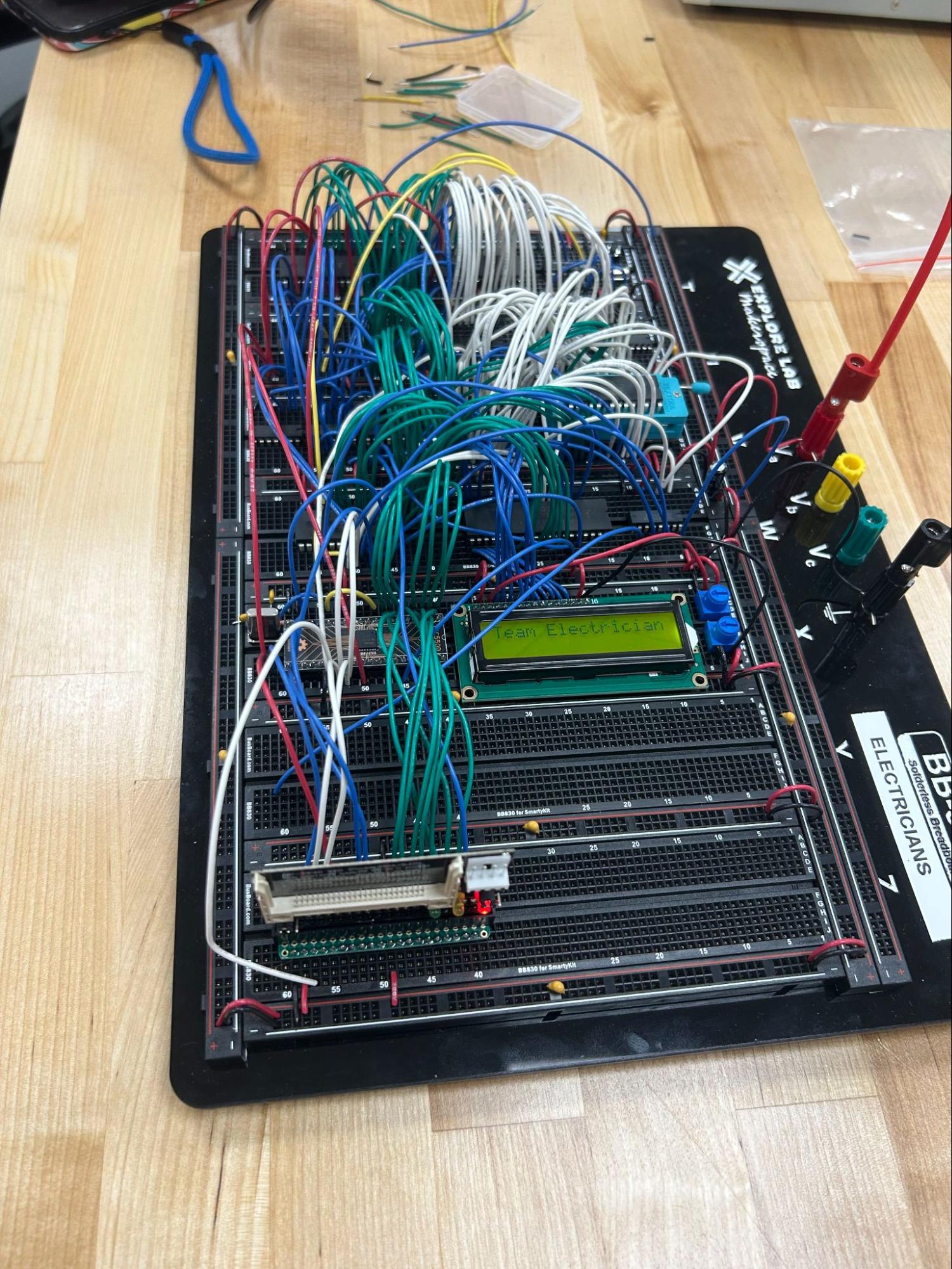
To verify the setup worked, I programmed the ROM with a pre-written “Hello, World” program. After removing the ROM chip, placing it in a programmer, and writing the program to it, I reinserted the chip and powered on the computer. “Hello, World” appeared on the LCD.
Interrupt Control
It was time to change the breadboard from a simple programmable device into something resembling a real PC. First up was a programmable interrupt controller. Interrupts allow the processor to pause its current program and handle more important tasks, critical for multitasking and I/O operations. Since there were multiple interrupt sources but the processor only has one interrupt pin, the controller managed which interrupt gets serviced. After installing the chip and wiring power, control signals, and address lines, I verified the computer still functioned with this addition.
Programmable Timer
Next came a programmable timer that sends regular interrupt signals, needed to implement a scheduler that can switch between different tasks. I wired it similarly to the interrupt controller, including clock signal connections to keep operations synchronized. Another power-on test confirmed everything still worked.
Serial Communication
The serial port was my favorite addition. It manages data transfer between the computer and external devices. With this in place, I could connect a modern PC and view output on a terminal emulator. This chip required several capacitors and resistors, plus another crystal oscillator for stable clock generation. After connecting the clock signal, adding data, address, and control wires, and wiring another interrupt line, I tested the system again. Everything still worked.
Persistent Storage
I installed a CompactFlash card connector using a design similar to older IBM PCs to provide persistent storage. This required a connector, numerous data wires, control wires, and connections to the interrupt timer. After inserting the CompactFlash card and powering on, a light on the connector confirmed it was receiving power and communicating with the system.
Speaker
The final hardware component was a small speaker with a few capacitors, resistors, and a driver chip. After installation and connecting it to the clock signal, powering on the computer produced a satisfying pop from the speaker, confirmation that audio output worked.
Booting from Disk
With all hardware in place, it was time to make the computer boot from storage rather than running fixed programs from ROM. I connected a USB adapter to enable communication with a PC, then programmed a BIOS (Basic Input/Output System) file to the ROM chip using the memory programmer from earlier labs. On my laptop, I installed PuTTY, a terminal emulator, and configured it to communicate with the breadboard computer through the serial connection. When I powered on the computer the BIOS performed its POST (Power-On Self Test), then proceeded to a memory check, verifying that all RAM functioned correctly. When I pressed the reset button, subsequent POST tests ran much faster since memory had already been validated since it’s booting from disk. The computer was now capable of booting an operating system from the CompactFlash card.
Conclusion
What started as an empty breadboard became a fully functional computer. A system with a CPU, memory, I/O capabilities, persistent storage, and the ability to boot from disk and run arbitrary programs. Along the way, I gained hands-on understanding of how computers work at the hardware level. I learned how clock signals synchronize operations, how memory addressing works, how interrupts enable multitasking, and how all these components communicate through carefully designed signal protocols. The complete computer represented hundreds of individual wire connections, multiple integrated circuits working together, and hours of careful assembly and debugging. I want to thank Dr. Kevin Angstadt for his guidance through this project and his help with very tedious debugging.